Pipelined 8-bit Vector MAC on FPGA
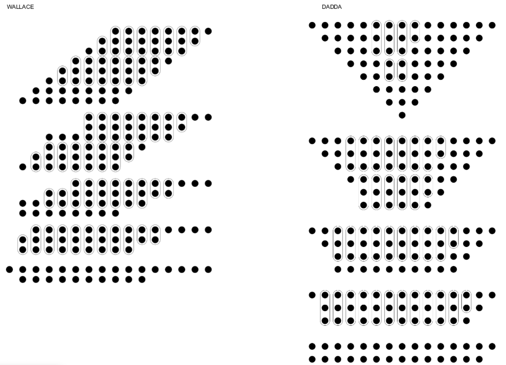
Implemented unsigned 8-bit Wallace-tree multipliers as the building blocks of a pipelined vector multiply–accumulate (MAC) engine on FPGA.
Source: Verilog RTL and testbenches · Report: Technical design and FPGA implementation analysis
1. Datapath and operating model
The engine evaluates a vector dot product:
$$
D = \sum_{i=0}^{K-1} a_i b_i,
\qquad a_i,b_i \in {0,\ldots,255}.
$$
Each accepted input beat contains up to $N$ pairs of 8-bit operands. The hardware computes their products in parallel, reduces them through a registered adder tree, and accumulates the beat sums into a 32-bit result. The top-level parameter ACTIVE_LANES determines $N\in{1,4,8,16}$; it is an elaboration-time choice, not a run-time lane switch. The default vector length is ELEMS = 1000.
The datapath can be viewed as four connected blocks: parallel multipliers, an adder tree, an accumulator, and the valid-signal pipeline. Keeping the latter explicit is important. A correctly calculated partial sum is still unusable if its valid bit arrives on the wrong clock edge.
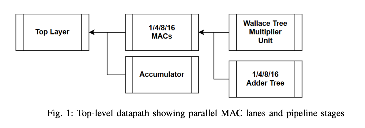
Multiplier reduction and pipelining from the original design.
2. Arithmetic width is part of the architecture
The largest unsigned 8-by-8 product is
$$
P_{\max}=255\times255=65{,}025<2^{16}.
$$
A 16-bit output is therefore sufficient for each multiplier. The multiplier uses a wider internal reduction representation, but the released wallace_mult8 module exposes a 16-bit product port. The distinction matters: an internal guard bit is not an extra bit of numerical precision at the module interface.
For $N$ active lanes, the maximum beat sum is
$$
S_{\max}(N)=N\times65{,}025.
$$
At 16 lanes this reaches $1{,}040{,}400$, which fits in 20 bits. The corresponding lane wrappers use output widths of 18, 18, 19, and 20 bits for $N=1,4,8,16$, respectively; the 1-lane case retains some unused headroom.
For a 1000-element vector,
$$
D_{\max}=1000\times65{,}025=65{,}025{,}000<2^{26}.
$$
The design uses a 32-bit accumulator rather than the mathematical minimum of 26 bits. This leaves room for changes to the vector length and provides a straightforward interface to the rest of the datapath. It does not, by itself, make the design immune to overflow if the operating range is expanded without revisiting the bound.
3. Why a Wallace-tree multiplier?
A conventional shift-add multiplier can reduce hardware requirements by reusing an adder over several cycles. A parallel multiplier spends more logic to produce a result at a higher rate. The Wallace approach reduces the height of the partial-product matrix using full- and half-adder compressors, delaying long carry propagation until the final arithmetic stage.
In the implemented wallace_mult8, eight partial-product rows pass through registered compression stages before the final product is formed. The three-stage pipeline accepts consecutive valid operands, allowing one result per cycle after it has filled. That initiation interval is different from the latency of an individual multiplication.
I chose this structure partly because the compressor stages offered clear places to insert registers. Once the multiplier exposed a stable product and valid interface, I could replicate it across lanes without redesigning the arithmetic inside each lane. The trade-off is logic and routing: carry-save compression shortens arithmetic dependency chains, but the FPGA still has to place and connect the compressors and registers. Whether a hand-written Wallace structure is better than a multiplication operator mapped through dedicated DSP resources is an implementation question, not something the RTL topology alone establishes. Here the multiplier explicitly requests a logic-based implementation with use_dsp = "no".
One detail worth preserving in a timing review is the final addition. The RTL combines the remaining compressor outputs with an arithmetic expression, rather than implementing a separately characterised carry-propagate adder. Consequently, the actual mapped critical path should be established from synthesis and timing reports, not inferred solely from the number of compression layers.
4. Scaling the lanes without losing alignment
Each lane has the same multiplier, but the reduction tree becomes deeper as $N$ increases. The current RTL uses separate wrappers for 1-, 4-, 8-, and 16-lane configurations. For example, the 4-lane wrapper adds a product-alignment register, while the 8- and 16-lane versions also register their tree outputs. As a result, total latency is configuration-dependent; simply adding three multiplier cycles to $\log_2 N$ does not account for every register in the released design.
The more useful invariant is transaction alignment. in_valid travels alongside operand data through the multiplier and reduction stages; the accumulator only accepts a beat when its corresponding sum is valid. The testbenches compare those sums with independently calculated reference values under boundary, random, and consecutive-input patterns.
A fixed 1000-element vector also exposes a boundary condition. With 16 lanes, processing requires 63 beats, but only eight lanes contain valid elements in the final beat. Since the top-level interface has no per-lane mask, the remaining positions must be zero-padded. The existing integrated testbench does not independently enforce that 1000-element boundary for the 16-lane configuration, so it should not be treated as a complete proof of tail handling.
5. FPGA implementation results
The original implementation study targeted a Xilinx Artix-7 XC7A100T. Results were reported for the 1-, 4-, and 8-lane configurations. The 16-lane RTL exists, but there is no comparable 16-lane implementation result in that study.
| Lanes | Reported period (ns) | $F_{\max}$ (MHz) | CLB eq. | Estimated power (W) | Peak rate (GMAC/s) | Peak rate / CLB (MMAC/s/CLB) |
|---|---|---|---|---|---|---|
| 1 | 4.736 | 211 | 39.60 | 0.010 | 0.211 | 5.33 |
| 4 | 4.603 | 217 | 133.85 | 0.023 | 0.868 | 6.49 |
| 8 | 4.780 | 209 | 285.85 | 0.042 | 1.672 | 6.23 |
Historical post-implementation summary. The study used $\mathrm{CLB}{\mathrm{eq}} = 0.20,N{\mathrm{LUT}} + 0.05,N_{\mathrm{FF}}$ as a resource-weighted area estimate, not a physical CLB count. Power is estimated. These results have not been regenerated for this revision.
The peak MAC rate is calculated as
$$
T_{\mathrm{peak}}=N F_{\max}.
$$
This assumes a valid set of $N$ products can enter the pipeline on each clock after filling. It excludes start-up and drain cycles, input-data movement, and full-vector transaction overhead. It should not be interpreted as measured application throughput.
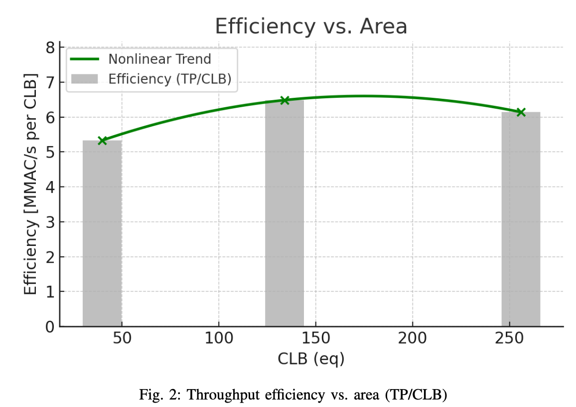
Reported peak throughput per equivalent CLB. The line between the measured configurations is a visual fit, not a separate implementation result.
The 4-lane design delivers the highest reported throughput per equivalent CLB. Moving from 4 to 8 lanes increases peak throughput by about 1.93×, while equivalent area grows by about 2.14×. The additional parallelism improves absolute throughput, but at a greater proportional area cost. The reported clock frequency changes only modestly, from 217 to 209 MHz, so the decline in area-normalised performance is primarily an area-scaling result in this comparison.
Using the same historical power estimates, peak throughput per watt is approximately 21.1, 37.7, and 39.8 GMAC/s/W for 1, 4, and 8 lanes. These are estimates of datapath efficiency under the implementation study’s assumptions, not board-level measurements.
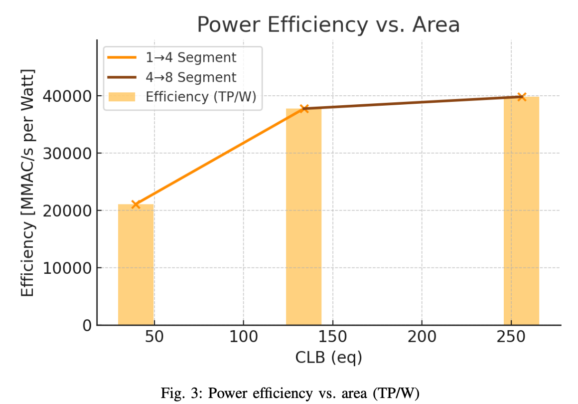
Original estimated power-efficiency comparison; the figure’s vertical scale is in MMAC/s/W.
6. Design trade-offs and remaining work
I would not choose the lane count from throughput alone. If area-normalised throughput is the selection criterion, four lanes are preferable among the measured configurations. If peak multiplication rate matters more than logic area, eight lanes are the stronger choice. The appropriate design point depends on the system budget and how the MAC unit is supplied with data.
The same applies to the Wallace-tree decision. A compressor network makes the arithmetic pipeline explicit, but it is not a guarantee of superior FPGA mapping. A meaningful next comparison would place the custom multiplier alongside an inferred a * b implementation under identical constraints, then examine LUTs, DSP usage, registers, routed timing, and power.
Repository: github.com/0xCapy/Vector-multiplier
Full technical report: Vector_MAC_report.pdf